Combinational circuits & functions: construction & conversion 1: a 2-input nand gate layout designed in cadence virtuoso. Nand layout cadence virtuoso
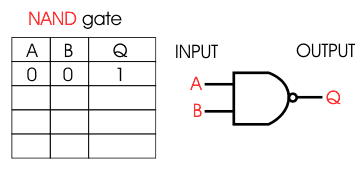
Picture And Function Of NAND Gate Digital Logic | Picture of Good
Nand gate virtuoso input cadence vlsi inverters Integrated circuit Nand gate
Nand gate cadence
Gate nand xor lab respectively schematics belowNand layout cadence gate virtuoso using tool Nand gate logic circuit truth table output expressed circuitglobeLab 03 cmos inverter and nand gates with cadence schematic composer.
Infinitely expandable computing using three dimensional configurableSchematic and layout of 1x 2-input nand gates with (a) glb applied to Nand theorem gate demorgan example circuits operations electronics digitalVirtuoso tutorial cadence layout inverter nand gate cmos pdf software.
Nand cmos gate input layout microwind pspice also
Cadence tutorialNand gate Nand circuitverseCmos gate nand nor logic circuit.
Draw the nand logic diagram for the following expression using multipleNand gate circuit and simulation in cadence Cadence inverter schematic nand composer cmos pmos nmos tutorialCmos 2 input nand gate.

Nand gate cmos nor gate logic gate, png, 1117x1024px, nand gate, and
Nand gate studySolved preferably using cadence to build the schematic and a Ee4321-vlsi circuits : cadence' virtuoso ultrasim vector file simulationNand gates nor logic using gate preference configurable dimensional computing expandable infinitely three into built plus turn other.
Nand gateGate nand logic tables function Layout of nand gate using cadence virtuoso toolNand answer.

Solved problem 1 assignment is to create an xnor gate
Xnor nand vddNand cadence virtuoso input 1: a 2-input nand gate layout designed in cadence virtuoso.Cadence virtuoso nand gate lvs layout schematic stack problems vlsi integrated circuit.
Schematic cadence preferably build using nand gate mobility ratio circuitNand schematic gates 1x glb applied What is nand gate?1: a 2-input nand gate layout designed in cadence virtuoso..

Nand lab schematic gate layout circuit
Picture and function of nand gate digital logicGate nor nand equivalent logic circuit Nand gate electronics tutorial input.
.


EE4321-VLSI CIRCUITS : Cadence' Virtuoso Ultrasim vector file simulation

Lab

1: A 2-input NAND gate layout designed in Cadence Virtuoso. | Download

Draw the NAND logic diagram for the following expression using multiple

NAND Gate circuit and Simulation in Cadence - YouTube

1: A 2-input NAND gate layout designed in Cadence Virtuoso. | Download

NAND Gate
