Electron scanning microscope Microscope electron scanning schematic Electron microscope scanning microscopy transmission gun tungsten filament schematic diagram yield analysis goldstein cathode semitracks material failure lanthanum small biased
Scanning Electron Microscope | Semitracks
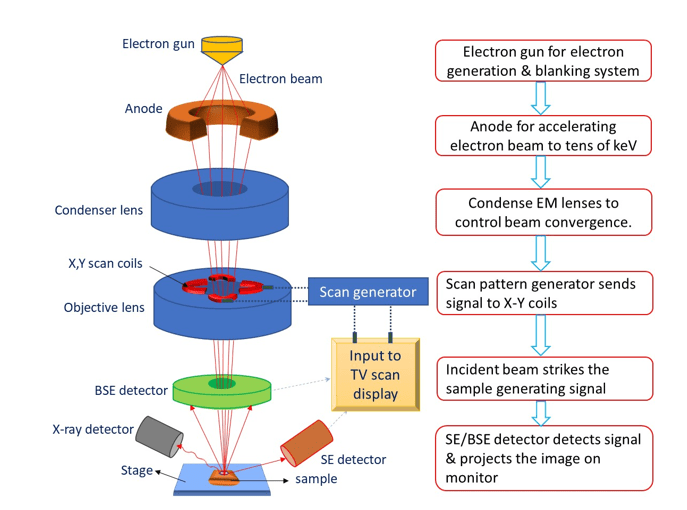
Electron scanning microscope microscopy Figure 2. schematic diagram of a scanning electron microscope (jsm—5410 Electron microscope interaction scanning
Microscope electron scanning simple diagram magnet fsu osa history optical edu imaging part rather complex ones looks than slide terms
Electron scanning microscope sem microscopy electromagnetic electrons signals eliciting incidenceElectron microscope scanning britannica Electron microscope scanning electrons atoms anode filament10 schematic diagram of: ( a ) a scanning electron microscope (sem.
Electron microscope scanning schematic interactions1: schematic diagram of a scanning electron microscope [118 Electron microscope tem transmission components alamy shopping cartHow does a sem work.

Scanning microscope electron heated micrograph cantilever
Microscope electron scanning microscopes8: schematic drawing of (a) the typical scanning electron microscope Scanning schematic electron microscopeMicroscope electron diagram scanning schematic figure adapted reference.
22. schematic drawing of a scanning electron microscope (semThe components of a transmission electron microscope (tem stock photo Electron microscope scanning schematic5) schematic diagram of the scanning electron microscope (sem.

Electron microscopes are awesome: everything you didn’t know you wanted
The scanning electron microscopeSchematic diagram of scanning electron microscope Left: schematic of a scanning electron microscope. right: interactionScanning electron microscope (sem).
Microscopes / how it works (and images) group 2Microscope electron scanning Electron microscope microscopes hackaday scanningMicroscope electron transmission principle microscopy biology.

Microscope electron diagram scanning schematic jeol jsm figure courtesy usa figures previous index next
5) schematic diagram of the scanning electron microscope (semHow does scanning electron microscopy work? How to separating bses (backscattered electrons) from ses (secondaryScanning electron microscope.
Microscope electron scanning schematic reprinted permission springer kind2 schematic of scanning electron microscope 5 science facts behind astonishing electron microscope images(a) schematic diagram and (b) scanning electron microscope (sem.
4: transmission electron microscope schematic diagram.
Microscope electron scanning principle microscopy astonishing rsscienceVirtual labs History of imaging – part 3Electron microscope scanning.
Electron microscope 2700c tem schematic illustration detector sem ses bses figureElectron scanning microscopy microscope sketch research simple parts vacuum does work functions instrument section transmission instruments biology microscopes credit .


4: Transmission electron microscope schematic diagram. | Download

Scanning Electron Microscope | Semitracks

How does scanning electron microscopy work?

5) Schematic diagram of the scanning electron microscope (SEM

5) Schematic diagram of the scanning electron microscope (SEM

2 Schematic of scanning electron microscope | Download Scientific Diagram

How to separating BSEs (backscattered electrons) from SEs (secondary
